
Single image allows inspection of semiconductor defects
- Writerkrissadmin
- Date2020-02-10 00:00
- Hits114
Single image allows inspection of semiconductor defects
- Real-time measurement technique developed for 3D nanodevices -
The Korea Research Institute of Standards and Science (KRISS, Acting President Seong-Jai Cho) succeeded in single-shot inspection of inner defects of advanced semiconductors and displays.
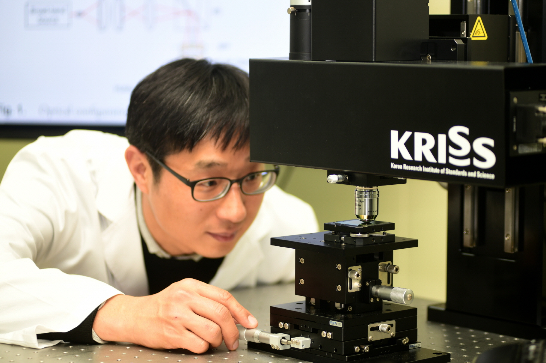
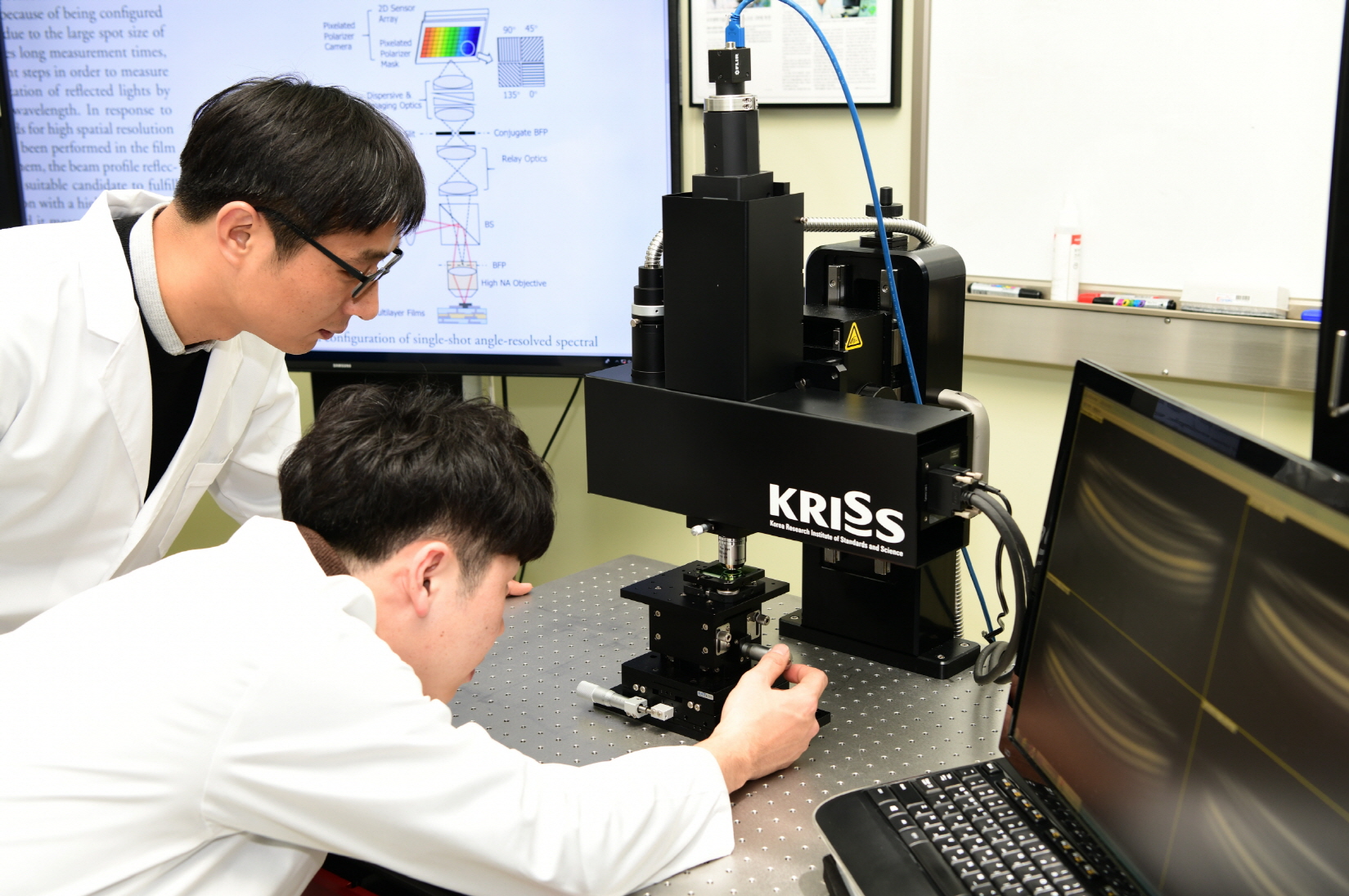
▲ Principal researcher Young-Sik Ghim of the Advanced Instrumentation Institute in KRISS is measuring a 3D nanodevice.
The team, led by principal researcher Young-Sik Ghim of the Advanced Instrumentation Institute, developed a technique to instantaneously determine structures and properties of 3D nanodevices in the production line. It is expected to enhance product quality by detecting defects without delay, thereby maintaining productivity.
- The technique enables real-time defect detection by measuring the thickness and refractive index of multilayer devices.
The key to memory device technology is to stack as many devices as possible in a given 2D area. Multilayer 3D nanodevices comprised of more than ten layers were developed using packaging technology to overcome 2D limitations, achieving faster speed and larger capacity. Today, 3D nanodevices are being widely used in advanced industries, including semiconductors, flexible displays, and IoT sensors.
The enhanced performance of devices has resulted in higher defect rates due to the more complex processes involved. However, industries check for defects by destroying some end products instead of performing real-time inspection. This is because nondestructive tests are time-consuming, and easily influenced by vibration and other environmental changes.
Fast and accurate measurements are necessary as defects discovered in later stages can lead to product recalls and significant losses. This has contributed to the decreasing productivity and rising unit cost of 3D nanodevices.

▲ A image got from a measurement technique developed for 3D nanodevices
Principal researcher Young-Sik Ghim and his team developed a technique to simultaneously determine thickness and refractive index based on a single image of a 3D nanodevice. Thickness and refractive index are two factors that must remain consistent to secure a stable yield.
- The team developed a system comprised of an imaging spectrometer, polarizing camera, and objective lens. They simplified the complicated process of taking multiple measurements into a single measurement, and improved spatial resolution by at least ten times.
When a nanodevice passes through the measuring instrument installed in the production line, an interference pattern develops on the objective lens. Pattern analysis through the imaging spectrometer and polarizing camera reveals various information such as incident angle, wavelength, and reflectance and phase in relation to polarization state, which are used to calculate the final thickness and refractive index.
While non-destructive inspection of devices has mostly been conducted in laboratories, the proposed technique can be easily integrated in production lines and applied across industries. It is also expected to improve quality control by managing the thickness of advanced devices.
▲ Principal researcher Young-Sik Ghim of the Advanced Instrumentation Institute in KRISS is measuring a 3D nanodevice.
Principal researcher Young-Sik Ghim said, “The technique contributes to domestication of measuring instruments, which has become crucial considering Japan’s export curbs, and secures higher device yield. It will play a key role in advanced industries from 3D semiconductors to next-generation displays, and ultimately enhance Korea’s global standing.”
The results were published in Optics Express (IF: 3.561) and Optics Letters (IF: 3.886).
原文源自KRISS网站,版权归其所有。如有侵权,请联系,第一时间删除。